- 您现在的位置:买卖IC网 > Sheet目录308 > ADZS-21364-EZLITE (Analog Devices Inc)KIT EVAL EZ LITE ADDS-21364
ADSP-21362/ADSP-21363/ADSP-21364/ADSP-21365/ADSP-21366
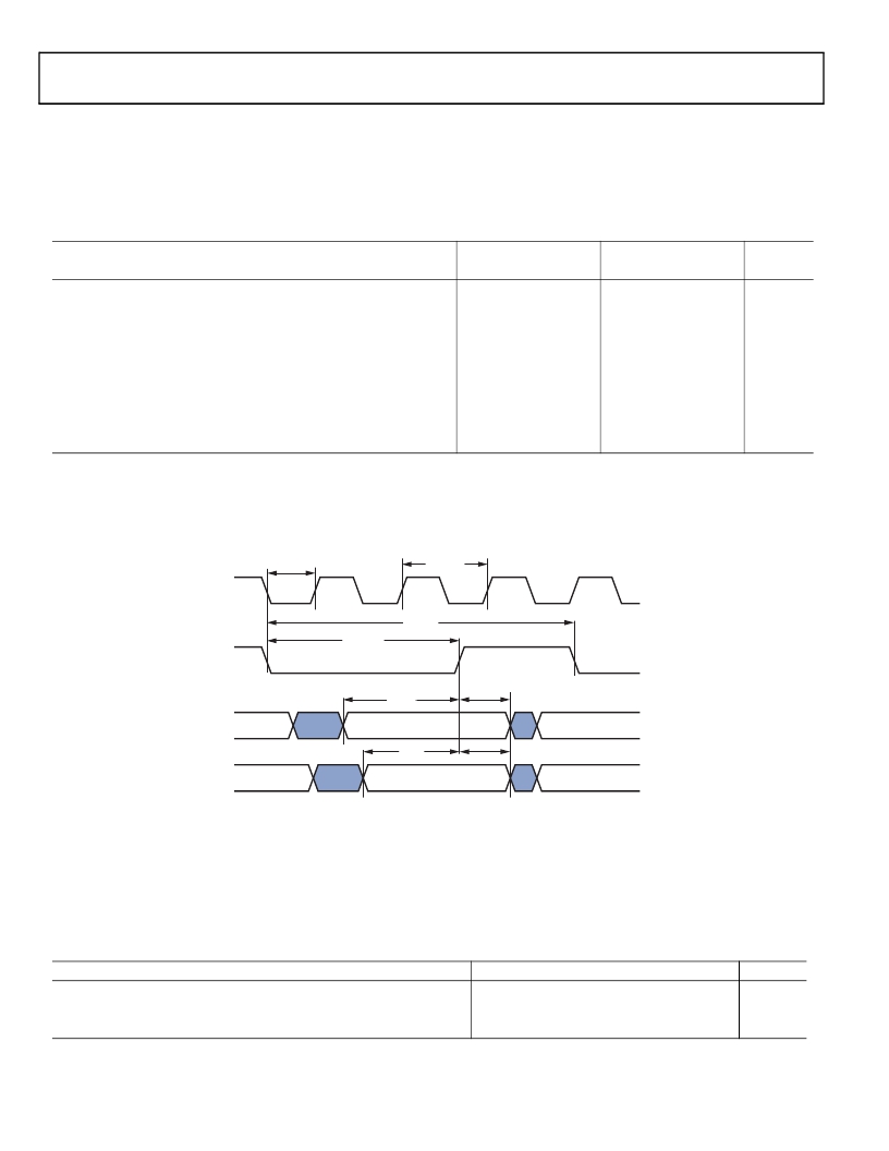
S/PDIF Transmitter Input Data Timing
The timing requirements for the S/PDIF transmitter are given
in Table 36 . Input signals are routed to the DAI_P20–1 pins
using the SRU. Therefore, the timing specifications provided
below are valid at the DAI_P20–1 pins.
Table 36. S/PDIF Transmitter Input Data Timing
K Grade
Y Grade
Parameter
Min
Max
Min
Max
Unit
Timing Requirements
t SISFS 1
t SIHFS 1
t SISD 1
t SIHD 1
t SITXCLKW
t SITXCLK
t SISCLKW
t SISCLK
Frame Sync Setup Before Serial Clock Rising Edge
Frame Sync Hold After Serial Clock Rising Edge
Data Setup Before Serial Clock Rising Edge
Data Hold After Serial Clock Rising Edge
Transmit Clock Width
Transmit Clock Period
Clock Width
Clock Period
3
3
3
3
9
20
36
80
3
3
3
3
9.5
20
36
80
ns
ns
ns
ns
ns
ns
ns
ns
1
The serial clock, data and frame sync signals can come from any of the DAI pins.The serial clock and frame sync signals can also come via PCG or SPORTs. PCG’s input can
be either CLKIN or any of the DAI pins.
SAMPLE EDGE
t SITXCLKW
t SITXCLK
DAI_P20–1
(TxCLK)
t SISCLK
t SISCLKW
DAI_P20–1
(SCLK)
DAI_P20–1
(FS)
t SISFS
t SISD
t SIHFS
t SIHD
DAI_P20–1
(SDATA)
Figure 32. S/PDIF Transmitter Input Timing
Oversampling Clock (TxCLK) Switching Characteristics
The S/PDIF transmitter requires an oversampling clock input.
This high frequency clock (TxCLK) input is divided down to
generate the internal biphase clock.
Table 37. Oversampling Clock (TxCLK) Switching Characteristics
Parameter
Frequency for TxCLK = 384 × Frame Sync
Frequency for TxCLK = 256 × Frame Sync
Frame Rate (FS)
Max
Oversampling Ratio × Frame Sync <= 1/t SITXCLK
49.2
192.0
Unit
MHz
MHz
kHz
Rev. J |
Page 40 of 60 |
July 2013
发布紧急采购,3分钟左右您将得到回复。
相关PDF资料
ADZS-21371-EZLITE
KIT EVAL EZLITE ADZS-21371
ADZS-21469-EZLITE
KIT EVAL EZ LITE ADSP-21469
ADZS-21479-EZLITE
KIT EVAL EZ BOARD ADSP-2147X
ADZS-21489-EZLITE
KIT EVAL EZ BOARD ADSP-2148X
ADZS-218X-ICE-2.5V
EMULATOR SRL FOR ADDS-218X-ICE
ADZS-BF506F-EZLITE
KIT EVAL EZLITE ADSP-BF506F
ADZS-BF518F-EZLITE
KIT EZ LITE BF512F/14F/16F/18F
ADZS-BF527-EZLITE
BOARD EVAL ADSP-BF527
相关代理商/技术参数
ADZS-21369-EZLITE
功能描述:KIT EVAL EZ LITE ADDS-21369 RoHS:是 类别:编程器,开发系统 >> 通用嵌入式开发板和套件(MCU、DSP、FPGA、CPLD等) 系列:SHARC® 产品培训模块:Blackfin® Processor Core Architecture Overview
Blackfin® Device Drivers
Blackfin® Optimizations for Performance and Power Consumption
Blackfin® System Services 特色产品:Blackfin? BF50x Series Processors 标准包装:1 系列:Blackfin® 类型:DSP 适用于相关产品:ADSP-BF548 所含物品:板,软件,4x4 键盘,光学拨轮,QVGA 触摸屏 LCD 和 40G 硬盘 配用:ADZS-BFBLUET-EZEXT-ND - EZ-EXTENDER DAUGHTERBOARDADZS-BFLLCD-EZEXT-ND - BOARD EXT LANDSCAP LCD INTERFACE 相关产品:ADSP-BF542BBCZ-4A-ND - IC DSP 16BIT 400MHZ 400CSBGAADSP-BF544MBBCZ-5M-ND - IC DSP 16BIT 533MHZ MDDR 400CBGAADSP-BF542MBBCZ-5M-ND - IC DSP 16BIT 533MHZ MDDR 400CBGAADSP-BF542KBCZ-6A-ND - IC DSP 16BIT 600MHZ 400CSBGAADSP-BF547MBBCZ-5M-ND - IC DSP 16BIT 533MHZ MDDR 400CBGAADSP-BF548BBCZ-5A-ND - IC DSP 16BIT 533MHZ 400CSBGAADSP-BF547BBCZ-5A-ND - IC DSP 16BIT 533MHZ 400CSBGAADSP-BF544BBCZ-5A-ND - IC DSP 16BIT 533MHZ 400CSBGAADSP-BF542BBCZ-5A-ND - IC DSP 16BIT 533MHZ 400CSBGA
ADZS-21369-EZLITE
制造商:Analog Devices 功能描述:ADZS-21369-EZLITE
ADZS-21371-EZLITE
功能描述:KIT EVAL EZLITE ADZS-21371 RoHS:是 类别:编程器,开发系统 >> 通用嵌入式开发板和套件(MCU、DSP、FPGA、CPLD等) 系列:SHARC® 产品培训模块:Blackfin® Processor Core Architecture Overview
Blackfin® Device Drivers
Blackfin® Optimizations for Performance and Power Consumption
Blackfin® System Services 特色产品:Blackfin? BF50x Series Processors 标准包装:1 系列:Blackfin® 类型:DSP 适用于相关产品:ADSP-BF548 所含物品:板,软件,4x4 键盘,光学拨轮,QVGA 触摸屏 LCD 和 40G 硬盘 配用:ADZS-BFBLUET-EZEXT-ND - EZ-EXTENDER DAUGHTERBOARDADZS-BFLLCD-EZEXT-ND - BOARD EXT LANDSCAP LCD INTERFACE 相关产品:ADSP-BF542BBCZ-4A-ND - IC DSP 16BIT 400MHZ 400CSBGAADSP-BF544MBBCZ-5M-ND - IC DSP 16BIT 533MHZ MDDR 400CBGAADSP-BF542MBBCZ-5M-ND - IC DSP 16BIT 533MHZ MDDR 400CBGAADSP-BF542KBCZ-6A-ND - IC DSP 16BIT 600MHZ 400CSBGAADSP-BF547MBBCZ-5M-ND - IC DSP 16BIT 533MHZ MDDR 400CBGAADSP-BF548BBCZ-5A-ND - IC DSP 16BIT 533MHZ 400CSBGAADSP-BF547BBCZ-5A-ND - IC DSP 16BIT 533MHZ 400CSBGAADSP-BF544BBCZ-5A-ND - IC DSP 16BIT 533MHZ 400CSBGAADSP-BF542BBCZ-5A-ND - IC DSP 16BIT 533MHZ 400CSBGA
ADZS-21371-EZLITE
制造商:Analog Devices 功能描述:ADZS-21371-EZLITE
ADZS-21375-EZLITE
功能描述:KIT BOARD FOR EZ-LITE ADSP-217X RoHS:是 类别:编程器,开发系统 >> 通用嵌入式开发板和套件(MCU、DSP、FPGA、CPLD等) 系列:SHARC® 标准包装:1 系列:PICDEM™ 类型:MCU 适用于相关产品:PIC10F206,PIC16F690,PIC16F819 所含物品:板,线缆,元件,CD,PICkit 编程器 产品目录页面:659 (CN2011-ZH PDF)
ADZS-21469-EZBRD
功能描述:KIT EVAL EZ BOARD ADSP-21469 RoHS:是 类别:编程器,开发系统 >> 通用嵌入式开发板和套件(MCU、DSP、FPGA、CPLD等) 系列:SHARC® 产品培训模块:Blackfin® Processor Core Architecture Overview
Blackfin® Device Drivers
Blackfin® Optimizations for Performance and Power Consumption
Blackfin® System Services 特色产品:Blackfin? BF50x Series Processors 标准包装:1 系列:Blackfin® 类型:DSP 适用于相关产品:ADSP-BF548 所含物品:板,软件,4x4 键盘,光学拨轮,QVGA 触摸屏 LCD 和 40G 硬盘 配用:ADZS-BFBLUET-EZEXT-ND - EZ-EXTENDER DAUGHTERBOARDADZS-BFLLCD-EZEXT-ND - BOARD EXT LANDSCAP LCD INTERFACE 相关产品:ADSP-BF542BBCZ-4A-ND - IC DSP 16BIT 400MHZ 400CSBGAADSP-BF544MBBCZ-5M-ND - IC DSP 16BIT 533MHZ MDDR 400CBGAADSP-BF542MBBCZ-5M-ND - IC DSP 16BIT 533MHZ MDDR 400CBGAADSP-BF542KBCZ-6A-ND - IC DSP 16BIT 600MHZ 400CSBGAADSP-BF547MBBCZ-5M-ND - IC DSP 16BIT 533MHZ MDDR 400CBGAADSP-BF548BBCZ-5A-ND - IC DSP 16BIT 533MHZ 400CSBGAADSP-BF547BBCZ-5A-ND - IC DSP 16BIT 533MHZ 400CSBGAADSP-BF544BBCZ-5A-ND - IC DSP 16BIT 533MHZ 400CSBGAADSP-BF542BBCZ-5A-ND - IC DSP 16BIT 533MHZ 400CSBGA
ADZS-21469-EZLITE
功能描述:KIT EVAL EZ LITE ADSP-21469 RoHS:是 类别:编程器,开发系统 >> 通用嵌入式开发板和套件(MCU、DSP、FPGA、CPLD等) 系列:SHARC® 产品培训模块:Blackfin® Processor Core Architecture Overview
Blackfin® Device Drivers
Blackfin® Optimizations for Performance and Power Consumption
Blackfin® System Services 特色产品:Blackfin? BF50x Series Processors 标准包装:1 系列:Blackfin® 类型:DSP 适用于相关产品:ADSP-BF548 所含物品:板,软件,4x4 键盘,光学拨轮,QVGA 触摸屏 LCD 和 40G 硬盘 配用:ADZS-BFBLUET-EZEXT-ND - EZ-EXTENDER DAUGHTERBOARDADZS-BFLLCD-EZEXT-ND - BOARD EXT LANDSCAP LCD INTERFACE 相关产品:ADSP-BF542BBCZ-4A-ND - IC DSP 16BIT 400MHZ 400CSBGAADSP-BF544MBBCZ-5M-ND - IC DSP 16BIT 533MHZ MDDR 400CBGAADSP-BF542MBBCZ-5M-ND - IC DSP 16BIT 533MHZ MDDR 400CBGAADSP-BF542KBCZ-6A-ND - IC DSP 16BIT 600MHZ 400CSBGAADSP-BF547MBBCZ-5M-ND - IC DSP 16BIT 533MHZ MDDR 400CBGAADSP-BF548BBCZ-5A-ND - IC DSP 16BIT 533MHZ 400CSBGAADSP-BF547BBCZ-5A-ND - IC DSP 16BIT 533MHZ 400CSBGAADSP-BF544BBCZ-5A-ND - IC DSP 16BIT 533MHZ 400CSBGAADSP-BF542BBCZ-5A-ND - IC DSP 16BIT 533MHZ 400CSBGA
ADZS-21479-EZBRD
功能描述:BOARD EVAL FOR ADZS-2147X RoHS:是 类别:编程器,开发系统 >> 通用嵌入式开发板和套件(MCU、DSP、FPGA、CPLD等) 系列:SHARC® 标准包装:1 系列:PICDEM™ 类型:MCU 适用于相关产品:PIC10F206,PIC16F690,PIC16F819 所含物品:板,线缆,元件,CD,PICkit 编程器 产品目录页面:659 (CN2011-ZH PDF)
